When a sensor delivers a signal in the millivolt range, something interesting happens: electronics suddenly stops being a mere intermediary and becomes the main character. A 0–20 mV signal is so small that, in an industrial environment, it almost feels like a whisper. It works, yes, but you have to listen very carefully.
The problem is that industry doesn’t run on whispers, but on robust, repeatable signals capable of traveling long distances through cabling without fading. This is where one of the great classics of instrumentation comes in: the 4–20 mA standard. It’s no coincidence that it has been used for decades. It is simple, resilient, and extremely practical.
In this article we will follow the complete journey of that tiny signal. The goal is to take a 0–20 mV input and transform it, step by step, into two useful outputs: a 0–10 V voltage output and a 4–20 mA current output. All of this is done with a modular analog architecture simulated in CircuitJS — clear enough to see each block separately while understanding how they all fit together in a single chain.
0–20 mV
0–10 V
1–5 V
4–20 mA
1) Problem Statement
At first glance, it might seem like this is simply a matter of amplifying the signal and calling it a day. But it isn’t. If you just multiply a small signal by a large number, you also multiply the noise, offsets, and any small imperfections that come with it. Designing a transmitter is not just about making the signal bigger — it’s about translating it into a language that the rest of the system can understand without ambiguity.
In this case, the transmitter has a dual purpose:
- to obtain a useful voltage output in the 0–10 V range,
- and to translate that same information into an industrial current signal of 4–20 mA.
In other words: we want to take a fragile signal and turn it into a serious process signal with proper industrial manners.
2) Input Stage: Filtering and Amplification
The input signal is modeled as a triangular wave between 0 and 20 mV. Before amplifying it, the signal passes through a first-order passive RC filter. This detail may seem minor, but it is not: amplifying a noisy signal is like zooming in on a blurry photo. You don’t fix anything; you just make the problem more obvious.
In the simulation, 10 kΩ and 100 nF are used, resulting in a cutoff frequency of approximately:
Since this frequency is much higher than that of the test signal, the filter barely affects the useful content. Its role here is not to “shape” the signal, but to clean it slightly so the rest of the circuit doesn’t have to work with high-frequency garbage.
Next comes the actual amplification. Instead of doing it all at once, it is split into two non-inverting stages:
- first stage with a gain of approximately 50.9, using 49.9 kΩ and 1 kΩ,
- second stage with a gain of approximately 9.9, using 8.9 kΩ and 1 kΩ.
This approach makes a lot of sense. Distributing the gain makes the system more reasonable, more stable, and closer to what you would actually build in a real design. The total gain is the product of both stages and brings the signal very close to the 0–10 V range.
If you had to summarize this stage in one sentence, it would be: we take an almost microscopic signal and bring it to a size we can work with without squinting.
3) Linear Scaling and Offset: From 0–10 V to 1–5 V
Here comes one of the most elegant tricks in the entire circuit. It might seem logical to send the 0–10 V signal directly to the current stage, but that would cause problems. With a sensing resistor of 250 Ω, a 10 V input would mean 40 mA — well outside the desired standard.
So the circuit does two things at once:
- compresses the range by multiplying by 0.4,
- and shifts it upward by adding 1 V.
The target equation for this block is:
This means a 0–10 V signal is converted into a 1–5 V signal. And that range is not chosen by chance: it is exactly what allows us to obtain a 4–20 mA loop when using a 250 Ω resistor.
Scaling
0–10 V → 0–4 V
Offset
0–4 V → 1–5 V
At its core, this block does something very typical of instrumentation: it not only changes the size of the signal, but also redefines its starting point. Thanks to that shift, the minimum is no longer 0 V but 1 V, which will later correspond to 4 mA.
4) Voltage-to-Current Conversion
The final stage is a current source controlled by an op-amp, an NPN transistor, and a sensing resistor. This is where everything fits together elegantly. The operational amplifier compares the control signal 1–5 V with the voltage drop across the emitter resistor \(R_{\text{sense}}=250\,\Omega\). The feedback forces a very simple condition:
And once that happens, the current is automatically set by a relationship that is almost impossible to argue with:
Therefore:
And that’s it. No magic. Just a combination of feedback, a well-chosen resistor, and the stubbornness of Ohm’s law.
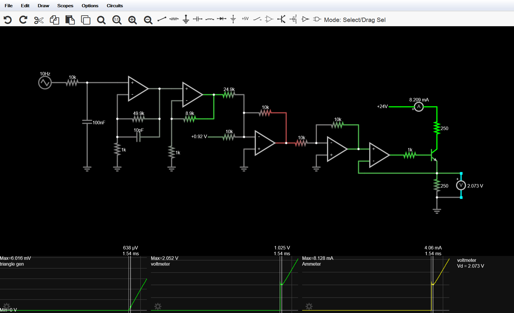
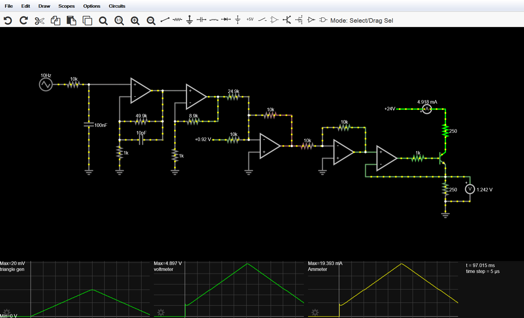
5) Real Simulation Results
So far everything sounds very clean, almost too clean. But the interesting part of a simulation is not confirming the ideal, but discovering how much the real circuit deviates from it. For this purpose, the minimum and maximum values observed in the scopes and meters were recorded.
| Magnitude | Simulated Minimum | Simulated Maximum |
|---|---|---|
| Sensor | 0 mV | 20 mV |
| 1–5 V Stage | 1.025 V | 4.897 V |
| Current Output | 4.06 mA | 19.393 mA |
The numbers already show that the circuit behaves as expected, although not perfectly ideally. And far from being a flaw, that is precisely what makes it interesting.
6) Real System Equations
Here comes one of the most satisfying parts of the analysis: taking the complete circuit with all its blocks and reducing it back to something as simple as a straight line. Because, seen from a distance, this transmitter is exactly that — a machine that converts a small variable into a larger one following a linear relationship.
6.1) Real conversion from 0–20 mV to 1.025–4.897 V
Using the points (0 mV, 1.025 V) and (20 mV, 4.897 V), the slope is:
The real straight line for this stage is:
That is: even when the sensor is at zero, the system already sits slightly above 1 V. This small offset will later translate into a quiescent current slightly above 4 mA.
6.2) Real conversion from 0–20 mV to 4.06–19.393 mA
Using the points (0 mV, 4.06 mA) and (20 mV, 19.393 mA), the slope is:
The final real straight line of the transmitter is:
And here’s something beautiful: all the complexity of the circuit ends up summarized in two numbers — a slope and a y-intercept.
7) Transmitter Sensitivity
In instrumentation, sensitivity is simply the slope of the transfer curve. It sounds solemn, but it really answers a very down-to-earth question: how much does the output change when the input changes a little?
In this case, the real sensitivity of the transmitter obtained in the simulation is:
Practical interpretation: for every 1 mV increase in the sensor signal, the output current increases by approximately 0.7667 mA.
It is not inherently a “good” or “bad” number. It is simply the natural consequence of having decided to map a 0–20 mV range onto a 4–20 mA range.
8) Comment on Deviations from the Ideal
If the circuit were perfect, the transmitter equation would be:
But what we actually obtain in the simulation is:
The differences are small, but they are there. And in fact, it would be suspicious if they weren’t. In a real build, these misalignments appear due to resistor tolerances, op-amp offsets, non-ideal saturations, and, in general, because the physical world doesn’t follow our schematics to the letter.
That is why industrial transmitters are calibrated. You adjust the zero, you adjust the span, and you accept that there is always a small negotiation between the circuit drawn on the board and the circuit that actually works on the bench.
9) Final Transmitter Error
Once the zero and gain are adjusted, the circuit achieves a full-scale error below 5%, which is perfectly reasonable for a conceptual, educational, and technical outreach implementation.
Taking the ideal upper end of 20 mA and the real maximum value obtained in simulation, the full-scale error is:
This result does not aim to compete with a high-precision industrial transmitter. What it demonstrates is something more important in this context: that the architecture works, that the overall linearity is preserved, and that the behavior is good enough to clearly explain how an analog 0–20 mV to 4–20 mA transmitter is built.
Conclusion
The interesting thing about this simulation is not only that it converts a millivolt signal into a standard current. The interesting part is that it allows us to see, almost without tricks, how a chain of very classic blocks — RC filter, non-inverting amplification, scaling with offset, and voltage-to-current conversion — ends up behaving like a well-defined linear relationship between the physical world and a transmissible signal.
With the values extracted from the simulation, the real transfer function of the transmitter is described by:
and its effective sensitivity is:
After calibration, the final error remains below 5% of full scale, so the transmitter can be considered acceptable for conceptual, educational, and technical outreach purposes. And perhaps that is the best way to summarize it: in the end, a transmitter is nothing more than a translator. It takes a small, delicate, and somewhat noisy physical reality and turns it into a robust signal that the rest of the system can understand without hesitation.
Note: the minimum and maximum images included in this article are captures from the simulation used to extract the real equations of the circuit.